Tci schematics

GBGRIDER

XS650 Enthusiast
Messages
82
Reaction score
0
Points
6
Location
Connecticut
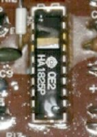
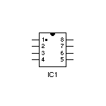
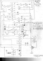
The only thing I was not able to do is get the internals on the rectangular transistors so I draw it as a box. Happy trouble shooting. If you have any questions I will try to answer them for you. SCHEMATICS ARE DOWN BELOW
 
Last edited:
That's a lot of work, but one thing makes me think you didn't check it thoroughly. On the IC chip you have 10 pins on one side and 8 on the other. And pin #1 isn't indicated. And I see power on it, but I don't see ground.
 
I got 10 pins on oneside and 8 on the other. Not sure what you are talking about. I would like to get it right and it took alot of time to do. Its pretty confusing i'll try to proof it with some fresh eyes tomorrow.
 
I don't know just how perfect it is, but it went in my folder with all the other wiring diagrams I have.
I have looked at several simple circuit boards, tracing the circuits on them looks to be an almost impossible task. On the TCI board it does look impossible.
I appreciate your time and dedication to do this tracing of the circuits. I'm sure your work will be appreciated by others too.
Leo
 
^Most pcb's are laid out automatically by giving a layout program a schematic file. I have no doubt there are programs that do the reverse, but I've never had to use one. But I have been assigned to reverse engineer this or that before.

One of the coolest things I've read along these lines is using the Photoshop flood fill feature to show all the connections to a trace. Just flood a trace in a photo and all the connections on it stand out in color:

http://busydizzys.com/index.php/201...op-to-aid-in-the-reverse-engineering-of-a-pcb

Don't file the tci schematic away just yet. Wait for the next rev or two. This one does have a couple probs. that will get ironed out I bet. I would like to see a data sheet for that IC chip but I spent hours trying to find it once. I always wished somebody at Yamaha or Hitachi would wikileak the tci folder....
 
I'll keep track of this thread and as changes occur I'll save the new diagrams as well.
Leo
 
Ok I look it over and it looks pretty good to me ill recheck it again later. Maybe you guys are not following the way i laid everything out. The triangles represent the wires coming in to the circuit board. White Green(WG) White Red(WR) Orange(O) Black(B) Black white(BW) Red White(RW). Black and Black White are your ground for the TCI. Now take a look at the transistor on the right with 10 pins at the top and 8 pins on the bottom. The bottom left pin reads R21 R20 which is resistor 21 and 20. Now look at the schematics and find R21 R20 and you well notice an arrow coming off of it. The arrow represents that bottom left pin. I tried to make it easier by doing this due to the fact there would be a ton more lines to follow. I Did notice i marked a transistor RTR it is supposed to be PTR. PTR is important transistor it supplies the negative for your primary coil. Alot of people find that to be the problem as i did when i trouble shot the circuit board. Please let me know it you see anything wrong i will change it i really want to get it right for everyone to trouble shoot from. Thank you
 
The thing with 18 pins isn't a transistor. It's a Hitachi HA1825P integrated circuit, probably some logic gate package.

Notice in the picture it has 9 pins on each side and that there's a notch in the top end of the package. The top pin on the left side of the notch is pin 1. The pin on the bottom right is pin 10. The top pin on the right side is pin 18.

When you draw a schematic the notch needs to be shown on the box, or at least some other obvious indication of pin 1. Then the other pins in the schematic need to be in the actual order they are in the physical chip. If there's a huge number of pins then each pin will be numbered in the schematic. But the pins are always in their actual physical order.

Ground and +V should always be indicated on the schematic at the chip too.

This isn't being picky. It's a universal convention that makes it understandable. The arrows and stuff are okay.
 

Attachments

  • pictureofxs650089.jpg
    pictureofxs650089.jpg
    119 KB · Views: 609
  • 8pindil.gif
    8pindil.gif
    480 bytes · Views: 700
ok you are differently right about that i know a little about logic control such as nor gates and gates in all that technical B.S. However my integrated circuit is lable OD2 HA1825p so i see what you are talking about. What year is your bike where you got that from? I got a 81. I'm going to look it up to see if i can find the internal of that integrated circuit board.
 
^Mine is an '81 too. I think it's the same in '80 and '81 and then in '82 I think they changed it some. If you can find a data sheet for the chip that will be a miracle. But maybe. The od2 on it is some kind of manufacturing code for internal use, maybe date of mfg, and the P on the end is the package type (in those days usually Plastic vs Ceramic).
 
Yea you are right about trying to find some data on that chip. All i got to say to the people using this to trouble shoot if everything checks out good it must be that damn chip. I use to have a computer problem to draw circuits i will try to find a new one just to make it neater plus i would like to put in the values of each resistor in tooo. It is kinda of weird that we have the same year and different stuff is yours a special too?
 
Great work both of you, it's all over my head. Careful of the gotcha monster. I think there were a fair number of different versions of the TCI internally beyond the 6 pin and 7 pin connector versions. I'll shoot some internal photos of the 4 or 5 I have.
 
Thats right i forgot about that, i have a 6 wire ignition setup i guess that would be pretty important information to tell people
 
The top left notch would be notch 1 and the bottom left will be notch 18

There's only one notch. If you look at the chip itself you'll see an actual notch in on the end. From that, you number the pins in the order I gave and that you see in the second picture. In the schematic, the chip should have something reprenting where that notch is and the pins should be in the right order. It doesn't take any explanation that way.

If this schematic is even only two-thirds right, you ought to go into something like electronics for a living. You have a talent for dogging it out. Most people would decide to do something else halfway through. It gets easier and better.
 
The chip looks right now, except that the pins are like mirror image as far as numbers go. If it was me I would put number 18 where number 1 is, and on down the line. Easy change to make. I would change them all to letters of the alphabet first, so it wouldn't be confusing. Then change the letters to the reversed numbers.
 
sorry I'm new to this forum I'm Mexican
I have a 1981 XS650 3G1 and I need to check the tci and pikcup diagram will have any such tci or some basis to repair it would appreciate in advance and the next week I'll upload my project carnal good post thanks
regards
:thumbsup::bike:
 
Thanks for posting the schematic. I have a 85 Virago 700.. (I know it is not as classic as the XS650 but, its what I have... at least it is a Yamaha).

Does anyone know of schematic for the Virago TCI? I have searched and searched... zip, nada, none.. I cant even find data in the IC chip in it. (M59201P).

I do have a parts list for the Virago TCI if anyone is interested.
 
Back
Top