sleddog83
XS650 Addict
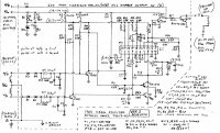
I have made some corrections to the 12-03 igniter schematic that I submitted previously. This igniter was off of a 83 Heritage Special SK. If you have any copies of the first version I submitted, get rid of them. This schematic was corrected using some reverse engineering methods.
Things to note: I suspect that the paired resistors R20/R21 and R22/R23 work with the tantalum capacitors C9 and C13 to produce a pair of integrator(ramp) waveforms. These waveforms are triggered by the pickup pulses P1 inverted through T2 and P2 inverted through T1. The pulses at the collectors of these two input transistors are positive going pulses. This is mostly speculation on my part since The IC on my igniter is dead. However comparing this igniter to an earlier one (12-01 igniter) I do see some similarities. What I thought originally might be fuses on the board, I now believe to be jumpers. The 12-03 igniter board is a single sided board with less components. Using a single side board required the use of a few jumpers on the component side.
From what I have read, the common failures of these boards are resistors R1, R2, Zener ZD1 which form part of the voltage regulation circuitry. The input diodes D1, D2, D3 and D4 are fairly low power diodes. The output transistor PTR also fails. Solder throughout the board , but especially at these components goes punky.
")